

When OpenAI’s GPT-4 was released in March 2023, the queues that formed were not for access to the model itself — they were in semiconductor fabrication facilities and logistics hubs in Taiwan, where NVIDIA‘s H100 GPUs were moving through supply chains with the urgency of wartime materiel. Technology executives from San Francisco to Singapore recall the same story: procurement teams authorising six-figure outlays for individual graphics cards, cloud providers rationing compute allocations, and board-level anxiety about whether a company’s AI ambitions might stall simply because it could not acquire the right silicon. NVIDIA, a firm founded to render video-game graphics, had become the single most consequential chokepoint in the global technology economy.
That chokepoint is now being deliberately dismantled — and the mechanism of its dismantling is a design philosophy that most people outside semiconductor engineering have never encountered: chiplets. Understanding what chiplets are, why they matter, and who is deploying them most effectively is rapidly becoming a core literacy for senior executives making capital-allocation decisions in the AI age.
The GPU Monoculture and Its Hidden Costs
NVIDIA controls approximately 80 per cent of the market for discrete AI accelerators. Its H100 GPU became the de facto standard for training large language models, with NVIDIA’s data centre revenue reaching $30.8 billion in a single quarter. The costs of this concentration manifest in three ways. First, pricing power: an individual NVIDIA H100 commands between $25,000 and $40,000; an eight-GPU server system routinely exceeds $250,000. Second, strategic dependency: NVIDIA’s CUDA parallel-computing platform has accumulated two decades of developer tooling creating formidable switching costs. Third, architectural lock-in: as NVIDIA integrates its Vera CPUs, Blackwell GPUs, and Spectrum-X networking into a single full-stack solution, customers who adopt each layer find it progressively harder to substitute any component.
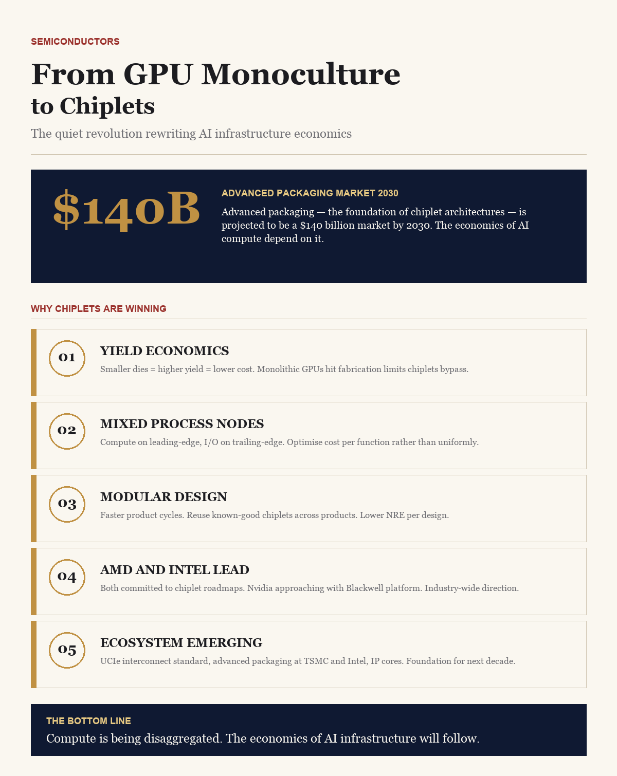
What Chiplets Are and Why They Change the Calculus
The conventional approach produces a monolithic die: a single large piece of silicon containing every function the chip needs. As die sizes grow, manufacturing defects become more likely, yields fall, and production economics deteriorate. Chiplet architecture solves this by decomposing the chip into smaller, specialised units manufactured separately — often on different process nodes — and then assembled into a single package using advanced interconnect technologies such as TSMC‘s CoWoS or Intel‘s EMIB. If one chiplet fails, only that smaller, cheaper component is discarded rather than the entire assembly.
AMD‘s MI300X demonstrated this commercially: it integrated CPU chiplets, GPU chiplets, and HBM stacks into a single package with 192 gigabytes of memory — 2.4 times that of the H100 — and 5.3 terabytes per second of bandwidth. The advanced packaging market enabling this integration is projected to grow at 18.6 per cent CAGR, reaching $14.8 billion. Apple’s M-series processors provide the most widely understood proof of concept: custom silicon designed for specific workloads delivers both better performance and better economics than general-purpose chips pressed into service.
Who Is Winning: The Challengers Taking Shape
Google’s sixth-generation TPU, Trillium, delivers approximately 926 teraflops of BF16 performance per chip — a 4.7-times improvement over the TPU v5e — with 67 per cent better energy efficiency. SemiAnalysis described Google’s TPU v7 programme as “the 900-pound gorilla in the room,” noting that its scale advantages compound with each generation.
AWS Trainium3, launched in December 2025, is AWS’s first 3-nanometre AI chip, delivering 2.52 petaflops of FP8 compute with 144 gigabytes of HBM3e memory. AWS cut its H100 cloud pricing by approximately 44 per cent in mid-2025 — a signal that competitive pressure from its own silicon was already feeding back into the market.
AMD’s MI300X secured a $100 billion procurement commitment from Meta as part of its diversification away from single-vendor dependency. The forthcoming MI400 systems offer HBM4 memory at 19.6 terabytes per second of bandwidth. AMD’s challenge remains the CUDA ecosystem’s accumulated tooling advantage, though its ROCm software stack continues to improve (see our analysis in The Taiwan Chokepoint).
Microsoft’s Maia 200 is reportedly migrating significant portions of OpenAI’s production traffic — including GPT-5 workloads — to internal silicon, providing a critical buffer against supply constraints. Intel is positioning its 18A process node as a fabrication alternative to TSMC for custom silicon programmes at Amazon and Microsoft (see our analysis in The $1.3T Chip Economy).
Implications for Enterprise Buyers and Investors
Alternatives to NVIDIA H100 clusters are typically priced 30 to 50 per cent lower on a raw hardware basis. For inference workloads — which represent the dominant compute cost for most enterprises deploying production AI — the price-performance case for alternatives is often stronger. AMD’s MI300X, with its large HBM pool, has proven specifically advantageous for large-model inference at scale (see our analysis in Edge Computing and IoT).
Enterprises that invest in hardware-agnostic software architectures preserve future optionality. Frameworks such as PyTorch and JAX abstract the hardware layer, and MLOps tooling increasingly supports multiple accelerator backends. Those that allow engineering teams to write directly against CUDA primitives are making an implicit bet on NVIDIA’s continued dominance.
For investors, the chiplet transition’s beneficiaries include TSMC and advanced packaging providers — which capture value regardless of whose chiplets they integrate — memory suppliers such as SK Hynix and Samsung whose HBM products are essential to every high-performance AI accelerator, and semiconductor IP companies such as Arm whose architectures underpin the custom silicon programmes at Amazon, Apple, and beyond.
India’s Strategic Position in the Chiplet Economy
India accounts for approximately 20 per cent of the global integrated circuit design workforce. Cadence Design Systems has an estimated 35 to 40 per cent of its global engineering talent in India. Samsung’s semiconductor research centre in Bengaluru has contributed more than 1,800 patents. Startup funding in India’s semiconductor sector grew tenfold in two years — from $5 million in 2023 to $50 million in 2025.
The chiplet transition matters specifically for India because chiplet architecture disaggregates the design problem. Rather than requiring mastery of an entire system-on-chip, it allows specialisation at the die level — areas where India’s VLSI engineering talent pool is deeply concentrated. India’s Semiconductor Mission 2.0 is explicitly targeting design capability alongside manufacturing. The Diplomat noted in March 2026 that India’s edge derives precisely from “skill at scale” — the ability to field thousands of trained engineers for complex verification and advanced packaging design tasks.
The Forward View
It would be a mistake to conclude that NVIDIA’s position is about to collapse. Its software ecosystem, systems integration capability, and the expanded multi-year partnership covering millions of Blackwell and Vera Rubin GPUs announced with Meta in February 2026 confirm that even the most committed alternative-silicon developers continue to need NVIDIA for frontier training workloads.
What is changing is the structure of the market around NVIDIA’s core. The plausible futures range from a bifurcated market — NVIDIA dominant in frontier training, chiplet-based custom silicon dominant in inference — to a more genuinely fragmented ecosystem where workload-specific accelerators capture substantial share of overall compute spend. The GPU monoculture is not ending quickly. But it is ending. Executives who recognise this early — diversifying silicon procurement, investing in hardware-agnostic architectures, watching the chiplet packaging supply chain — will find themselves with options their competitors have already foreclosed.